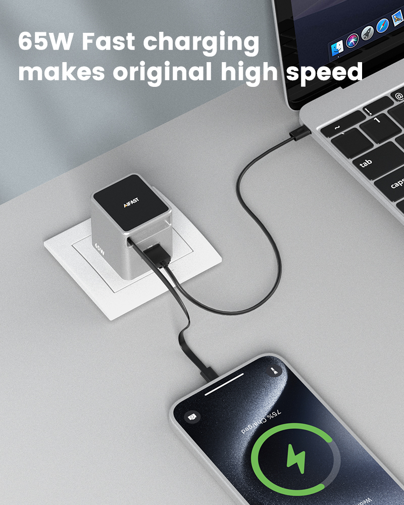
In the 2026 global consumer electronics market, the physical size of chargers has nearly reached the limits of power density. When USB-PD 3.1 protocols and 240W charging efficiency have become standard in high-end markets, product differentiation is no longer defined by industrial design or exterior aesthetics. Instead, it hinges on the hidden “heart” inside—the smart fast-charging PCBA (Printed Circuit Board Assembly).
For cross-border e-commerce leaders and global brand distributors, a charger’s success depends on three critical metrics: conversion efficiency, thermal management, and protocol compatibility depth. Based on ESC Technology (AOVOLT)’s core R&D team experience at major smartphone manufacturers like Xiaomi and OPPO, over 85% of after-sales returns and platform delisting risks stem from using outdated reference PCBA designs lacking dynamic power allocation logic.
This article delves into the technical selection logic behind high-performance smart fast-charging PCBAs and explains how they build competitive barriers for B2B partners through “original factory speed” and “ultra-low temperature” operation.
Why PCBA Is the “Soul” of Fast-Charging Products, Not Just a Component
Within the fast-charging supply chain, the PCBA determines both current stability and operational safety. Using low-end, highly commoditized reference PCBAs exposes brands to hidden costs:
Technical degradation and performance drop
Many commercial chargers claim 100W output. However, after 15 minutes of simultaneous multi-port operation, poor PCBA design often leads to overheating. The system automatically throttles current, dropping charging speed to 60% of the nominal value. Providing you with PPS Fast Charging 2026: Smart Power Supply B2B Guide.
Platform compliance risk
Major platforms like Amazon have entered a “chip-level” era of safety compliance. PCBAs lacking proprietary protocol control and fine-grained protection circuits often fail EMI (electromagnetic interference) testing, leading to entire product batches being delisted.
Brand reputation “heat expansion”
Consumer complaints about excessive heat are irreversible. AOVOLT’s “Original Speed” philosophy centers on simulating factory charging curves through self-developed PCBAs, ensuring full-load output while keeping temperature rise 5–8°C below industry standards.
Table 1: Comparison of Generic vs. AOVOLT High-Performance PCBAs
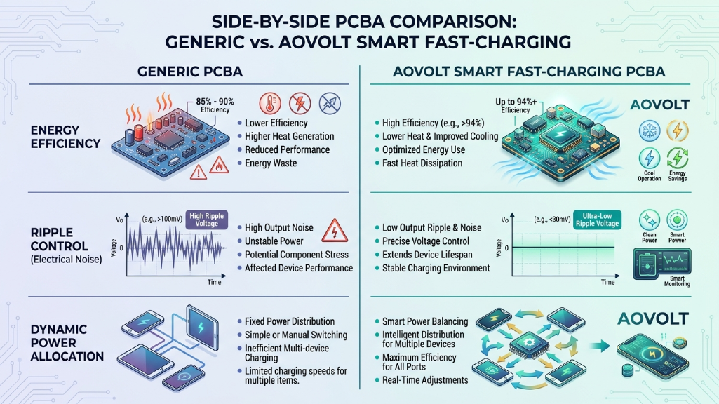
| Evaluation Metric | Generic Reference PCBA | AOVOLT Self-Developed Smart PCBA | Brand Benefits |
|---|---|---|---|
| Energy Conversion Efficiency | 88%–91% | 94.5%–96% (GaN Integration) | Reduces waste heat, enables more compact designs |
| Dynamic Power Allocation | Fixed split (e.g., 45W+20W) | AI-driven, demand-based (1W precision) | Protects battery life, optimizes multi-device charging |
| Ripple Control | <150mV | <50mV (factory smartphone standard) | Ensures touchscreen reliability, extends motherboard lifespan |
| Standby Power | >100mW | <30mW (latest Level 6 efficiency) | Meets the strictest global environmental standards |
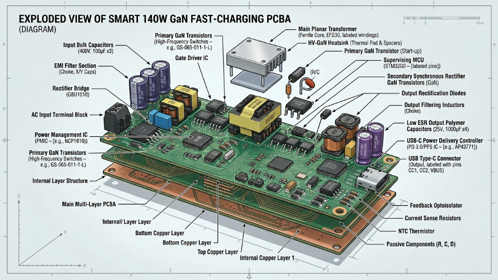
Deep Dive: Four Core Technical Pillars of High-Performance Smart Fast-Charging PCBAs
Experience working with Global 500 accessory brands shows that an outstanding smart fast-charging PCBA must excel across four engineering dimensions:
Deep Customization of High-Integration Power Management ICs (PMIC)
AOVOLT’s R&D DNA comes from top smartphone brands. To achieve “factory speed,” the PCBA’s main controller must be highly integrated. Self-developed fast-charging ICs enable deep compatibility with PD 3.1, PPS, QC 5.0, and various proprietary smartphone protocols. This ensures third-party accessories not only charge devices but also accurately interact with a phone’s internal fast-charging logic, preventing battery temperature spikes from overcurrent.
Extreme Thermal Management: Logic Behind Low Heat
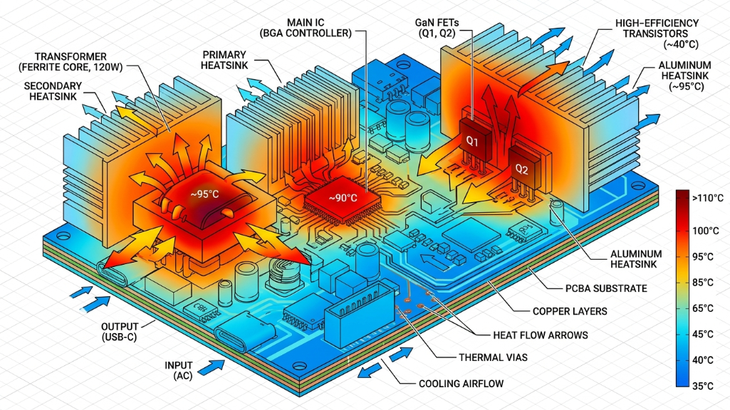
Heat is the enemy of high-performance fast charging. Leveraging deep expertise in third-generation GaN (gallium nitride) semiconductors, AOVOLT employs spatial separation on the PCBA, physically isolating high-heat transformers from protocol control circuits. High-frequency synchronous rectification (SR) further reduces diode losses, improving conversion efficiency at the source.
Data point: In a 25°C lab environment, the AOVOLT 140W PCBA exhibited a 12.5% lower temperature rise in key components than competing products after 2 hours of full-load operation.
Dynamic Power Allocation (DPA) 2.0
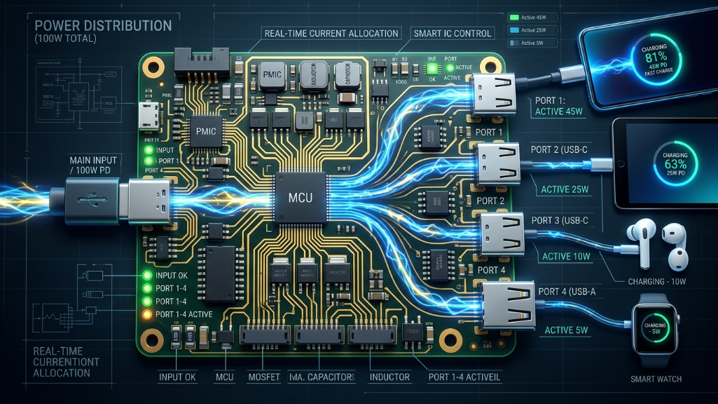
Multi-port desktop chargers are highly demanded in the B2B market. Traditional PCBAs often interrupt charging when a new device is connected. AOVOLT’s smart PCBA features “zero-second switching” logic, instantly redistributing current by detecting USB port load impedance in milliseconds, enabling uninterrupted, interference-free multi-device charging.
Multi-Layer Active Safety Architecture
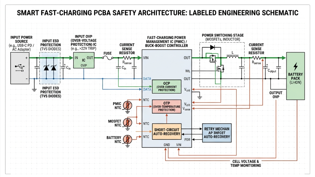
Compliance is not about sticking a CE label on a circuit; it requires redundancy in design.
-
OVP/OCP/OTP: Hardware-level protection against overvoltage, overcurrent, and overtemperature.
-
ESD protection: Critical interfaces equipped with high-spec ESD devices to handle static in varied climates.
-
Short-circuit auto-recovery: Smart detection of short circuits with automatic recovery within 0.5 seconds.
AOVOLT’s Core Competitiveness: Transforming Manufacturer R&D Genes into Brand Moats

Charging products are easy to make, but delivering a “perfect factory-like experience” is challenging. AOVOLT bridges the technology gap between third-party accessories and original smartphone brands.
Downward Compatibility to Smartphone-Grade Standards
Drawing on 15 years of experience at Xiaomi, OPPO, and Vivo, AOVOLT reconstructs power management logic rather than merely designing PCBAs.
-
Simulating factory curves: Many chargers drop current too sharply after 80% battery, prolonging the final 20% charging. AOVOLT algorithms improve trickle charging efficiency by over 20%.
-
Proprietary protocol support: Self-developed ICs enable hardware-level compatibility with mainstream brands, eliminating issues like “fast-charge icon not appearing” or handshake failure.
Patented Appearance and Structural Design: Avoiding Platform Delisting
For cross-border sellers on Amazon, Wayfair, and others, homogeneous designs bring compliance and infringement risks.
-
Exclusive patents: All AOVOLT products have unique appearance and structural patents.
-
Differentiated competitiveness: High-density vertical stacking reduces product volume by 15–20% at the same power level, creating a natural premium brand positioning.
Global Market Access: How PCBA Design Impacts Certification Compliance
In 2026, simple “assembly” no longer passes stringent compliance checks. PCBA layout directly affects EMI/EMC test outcomes. Industry data shows over 70% of fast chargers fail CE or FCC tests, mainly due to high-frequency switching interference. AOVOLT ensures 100% certification pass rates using:
-
Frequency Shuffling: Introduces PWM frequency jitter to disperse EMI peaks.
-
Four-Layer PCB Process: Includes an independent shielding layer, significantly improving interference resistance.
Table 2: Global Certification Requirements and AOVOLT Compliance
| Region/Market | Core Certifications | AOVOLT Coverage | B2B Procurement Focus |
|---|---|---|---|
| Europe (EU) | CE, RoHS, ErP (Level 6) | Standard on all products | Environmental materials, standby power |
| North America (NA) | FCC, UL, ETL, DOE | Full customization support | Electrical safety, fire rating (V0) |
| Global/Universal | IEC 62368-1, IEC 62133 | TUV/SGS certified | Telecom-grade safety, core power bank certification |
| Logistics/Transport | MSDS, UN38.3 | Essential for power banks | Air/sea compliance, port clearance |
Choosing a PCBA Partner: It’s More Than Price
For B2B decision-makers, unit price is just the tip of the iceberg. Poor-quality PCBAs incur high total cost of ownership (TCO).
Hidden Costs to Consider
Based on global distributor experience, focus on three “hidden value” dimensions:
-
Yield Rate: AOVOLT ISO9001-certified factory, 100% full-load aging and ATE testing, ensures >99.8% pass rate.
-
Supply Chain Stability: Strategic agreements with core chip suppliers guarantee timely OEM/ODM delivery even in peak season.
-
Secondary Development Capability: Custom PCBA revisions or prototypes completed in 7–14 days per brand requirements.
FAQ: Smart Fast-Charging PCBA
Q1: How does AOVOLT prevent “instant disconnects” when multiple devices connect?
A: Traditional PCBAs delay power redistribution. AOVOLT’s “Smart-Power-Stream” algorithm completes the switch in <50ms, virtually unnoticed by users, protecting sensitive devices like laptops.
Q2: Why do some GaN chargers still overheat?
A: GaN is just a material; thermal design is key. Overcrowded PCBA layouts trap heat at transformers and main ICs. AOVOLT uses patented thermal potting or large copper heat sinks with optimized PCB traces for even heat dissipation.
Q3: Does the PCBA support firmware upgrades (OTA)?
A: Yes. High-end stations and power banks have data interfaces for future protocol updates, preventing obsolescence.
Q4: Can AOVOLT provide full-chain certification support from PCBA to finished product?
A: Absolutely. Our PCBA designs comply with strict international standards from the outset, enabling rapid acquisition of local market certifications.
Conclusion: Driving Brand Value Through Core Technology
In today’s mature fast-charging market, survival and profitability belong to brands with strong technical moats. Partnering with ESC Technology (AOVOLT) for PCBA design and manufacturing provides not just a circuit board, but a mature, factory-validated, patent-protected power management ecosystem.
From “factory-level” charging speed to “low-temperature, heat-free” safety, AOVOLT leverages PCBA innovation to create differentiated competitive advantages for global distributors and brands.
Ready to upgrade your product line?
[Contact AOVOLT’s senior engineering team to get your customized fast-charging PCBA blueprint.]
References: