In the consumer electronics field, 140W is no longer just a number. It signifies achieving high-density energy conversion within an extremely compact physical space while ensuring safety. Regarding 140W PD3.0 fast charging PCBA design solutions, we have witnessed countless design-level challenges. Many PCBA solutions on the market lose control of temperature rise under full-load testing, or experience charging interruptions due to protocol stack redundancy during compatibility handshakes. Our core conclusion is straightforward: if you cannot address thermal management and full protocol compatibility at the source, any gimmicks in appearance design are castles in the air. For B2B clients, what we deliver is not merely a circuit board but a complete, rigorously tested, full-protocol-compatible mass production solution, enabling your product to capture the market in a very short time.
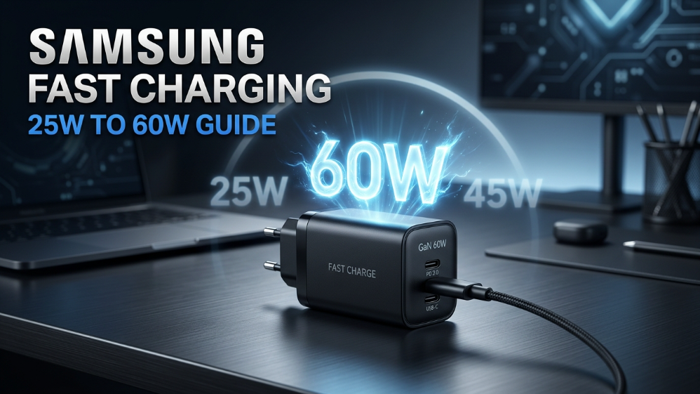
Core Technical Challenges in 140W Fast Charger PCBA Design
Achieving High Power Density Through Advanced GaN Integration
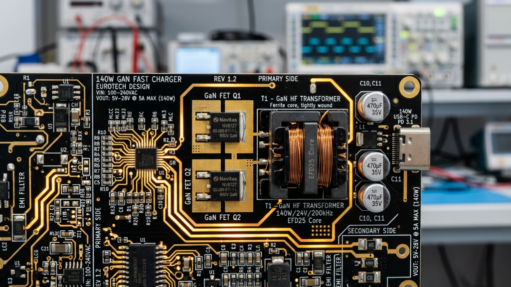
To achieve 140W power density, traditional silicon devices have reached their physical limits. Switching to GaN (Gallium Nitride) fast charger architecture is the only viable choice. Gallium Nitride’s excellent switching frequency reduces losses, but it also imposes extremely high demands on PCB routing. In our R&D lab, we refuse to use generic topologies. We found that by optimizing transformer winding processes in combination with high-frequency magnetic materials, the volume of the heat-generating core area can be reduced by more than 30%. This is not just a matter of material selection; it is a design philosophy.
Thermal Management Strategies for High-Wattage Output
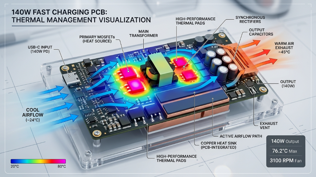
At high power output, heat is the number one killer of products. For high power density thermal management, we employ a multi-dimensional cooling mechanism. It is not just about adding aluminum heat sinks; through precise thermal field simulation of heat sources such as MOSFETs and synchronous rectifiers, we deploy thermal pads at critical points and form conduction paths with the PCBA enclosure structure. We are not seeking the upper limit of cooling; we are pursuing a logical closed-loop of thermal balance.
The table below shows comparative data for 140W output efficiency under different technical architectures:
| Technical Dimension | Traditional Silicon Architecture | GaN Optimized Solution | Our Core Advantage |
|---|---|---|---|
| Conversion Efficiency | 88%-90% | 94%-96% | Lower heat, higher reliability |
| Volume Ratio | 100% (baseline) | 65% | Minimalist appearance, suitable for handheld design |
| Heat Distribution | Spot intense heating | Uniform planar conduction | Prolongs component lifespan |
| Protocol Compatibility | Supports mainstream PD only | Supports all protocols (QC/SCP/PPS/Apple) | Full multi-protocol support |
Ensuring Seamless Multi-Protocol Compatibility
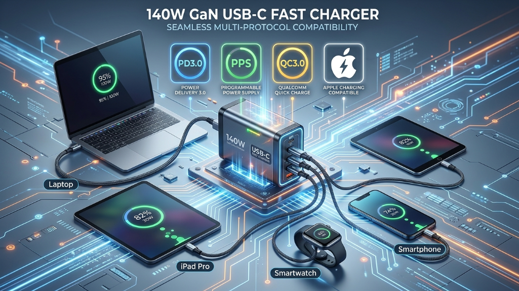
This is often the overlooked deep-water zone in B2B procurement. Multi-protocol fast charging compatibility is not just a label. When developing the 140W solution, we focused on full protocol logic. If a PCBA does not perfectly switch between PD3.0, PPS, QC3.0, FCP, SCP, AFC, Apple 2.4A, and BC1.2, after-sales issues will become a nightmare in global cross-border e-commerce. We understand that microsecond-level delays in protocol handshakes can trigger protection mechanisms. Therefore, our firmware is optimized for full protocol support, ensuring seamless fast charging for devices from different brands. This deep adaptation is the technical foundation enabling us to support high-end clients’ global deployment.
Bridging the Gap: From PCBA Prototyping to Mass Production
Often, a gap exists between the “prototype” in the lab and the “mass production unit” in the factory. A common industry phenomenon is the disconnection between PCBA solution providers and assembly factories. This leads to structural limitations not being considered during PCBA design or cooling space being compromised during mold injection due to poor internal layout. This is precisely why AOVOLT, over its 15-year manufacturing history, chose to pursue a heavy-asset, vertically integrated path.
The Critical Role of Vertical Integration in Quality Control
True custom PCBA manufacturing capabilities should not be limited to the circuit board itself but require control over the entire supply chain. We have a full closed-loop production line, from design, mold opening, injection molding to hardware integration. This means when designing the 140W PCBA, our structural engineers have already preset the heat dissipation channels in the injection-molded enclosure. Through vertical integration, we can control component tolerances at the micrometer level, ensuring that strict quality control (QC) is not just a slogan on the wall but a tangible fact on every production line.
For brands pursuing high-end customization, the greatest value of this integration is that you no longer need to source solutions from one provider and molds from another. We offer one-stop technical transformation, greatly compressing the cycle from design to market. Provide you with safe fast charging PCBA wholesale: 140W GaN guide.
Custom Sourcing: Why Design and Manufacturing Must Align
For brands targeting the mid-to-high-end market, a highly recognizable appearance design is a competitive moat. However, such recognition often requires complex mold processes. When handling various irregular and thin product designs, through deep collaboration with the circuit R&D team, we resolve the conflict between “high power” and “artistic appearance.” We are not only manufacturers but also technical consultants for your product line, ensuring every 140W charger leaving the factory achieves both peak performance and aesthetic appeal.
| Manufacturing Service Dimension | Ordinary Solution Providers | AOVOLT Vertical Integration |
|---|---|---|
| Design Fidelity | Dependent on third-party cooperation | Original factory closed-loop, precise mold/injection fidelity |
| Production Lead Time | Long (multi-party coordination) | Rapid delivery (own factory) |
| Quality Traceability | Partially visible | Full-chain digital traceability |
| Cost Control | Multiple markups | Source manufacturing, optimal cost-performance |
How to Evaluate an OEM/ODM Partner for 140W Fast Charging Solutions
When selecting a manufacturing partner, you need to assess not their ability to “paint promises” but their practical experience in 140W USB-C PD circuit design.
Assessing R&D Expertise and Industry Experience
A source factory with 15 years of experience means we have gone through every iteration from QC2.0 to PD3.0, from silicon-based to GaN. Facing complex global market demands, we have accumulated not only technical parameters but also deep knowledge of different countries’ safety standards and various end-device charging logics. Such experience cannot be quickly compensated by a start-up by merely adding R&D staff.
Lead Time, Cost Efficiency, and Customization Capabilities
As an OEM/ODM power bank manufacturer, our logic is simple: respond to the rapidly changing market through fast lead times and reduce inefficiencies through source integration. For procurement managers seeking high-quality factories, stable capacity and controllable delivery times are the cornerstone of supply chain security. Our full-matrix product line—from power banks and magnetic charging banks to desktop fast chargers—can all be rapidly customized based on the same mature 140W solution.
Frequently Asked Questions (FAQ)
Q: Is the 140W PCBA solution compatible with all types of laptops?
A: Yes. Based on our fully protocol-compatible logic, the solution automatically identifies and adapts to major laptop brands’ PD3.0 and proprietary fast charging protocols, ensuring the highest efficiency charging experience.
Q: How does AOVOLT ensure PCBA yield during mass production?
A: We utilize fully automated SMT lines and multiple burn-in tests. Combined with vertically integrated injection molding and mold support, functional testing is completed before assembly, ensuring extremely high end-product yield.
Q: Can we customize special charging protocols according to our requirements?
A: Yes. With deep firmware development capabilities, we can flexibly modify and adapt protocols for specific regional market needs or brand requirements.
Q: How to ensure thermal safety of a 140W solution while pursuing a slim design?
A: By optimizing internal layout and thermal conduction materials, we isolate or efficiently conduct heat from hotspots to the enclosure, ensuring products meet safety standards even under full-load operation.
Q: How long does it typically take from design confirmation to product delivery?
A: With our full mold and injection closed-loop capabilities, we can shorten delivery cycles by at least 30% compared to traditional OEM models. The exact time depends on product complexity; we welcome direct discussion of your detailed requirements.
Conclusion
In the uncertain global trade environment, finding a partner who understands cutting-edge technology and possesses heavy-asset manufacturing capabilities is often key to a brand’s long-term strategy. From PCBA circuit design refinement to full-product manufacturing craftsmanship, AOVOLT is committed to providing global brands with reliable mass production solutions. Whether you are conceptualizing a new high-performance charging product or upgrading your existing product line’s technical specifications, we are ready to provide necessary support through in-depth technical evaluation and customized services. If you wish to explore how to integrate these high-performance solutions into your next-generation product line, we can discuss the details extensively.
References: