Stop wasting time with resellers. Go straight to the source factory and inspect the PCB assembly skills at the base level. For B2B buyers and cross-border product managers currently sourcing, here’s the bottom line: currently in the manufacturing hub of Dongguan, bare 140W PCBA boards using top-tier GaN (Gallium Nitride) core components typically wholesale for $12–$18 per unit in bulk (depending on whether you choose IC solutions from Navitas, Innosilicon, or PI). If you require a full turnkey project with high-end customized OEM chargers, a reasonable ex-factory Aurora price should range from $25–$35. Any cooperation discussed outside of this cost baseline risks either being overcharged by multiple outsourcing layers or getting low-quality boards using recycled components that can fail.
Selecting products is not like buying a blind box. A qualified PD3.1 power adapter supplier’s core competitiveness always lies in the hardware’s foundational design.
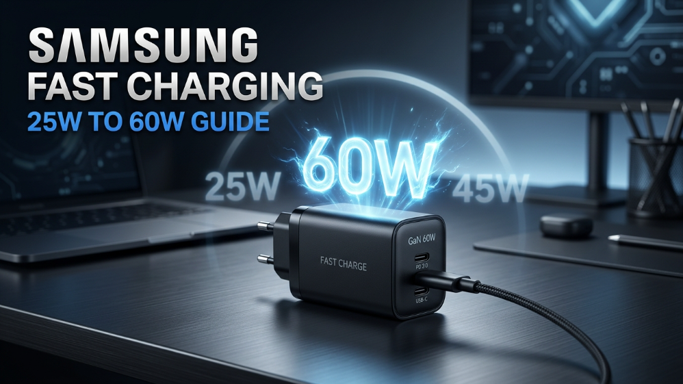
The Rise of 140W Fast Charging: Why Multi-Protocol PCBA is Core
Meeting the Extreme Demands of Modern High-Power Devices
The 65W and 100W era is over. Ever since Apple implemented the 28V/5A power delivery standard on the MacBook Pro 16-inch, the power ceiling of the consumer electronics market has been completely raised. High-power charger PCB assembly is no longer just stacking components.
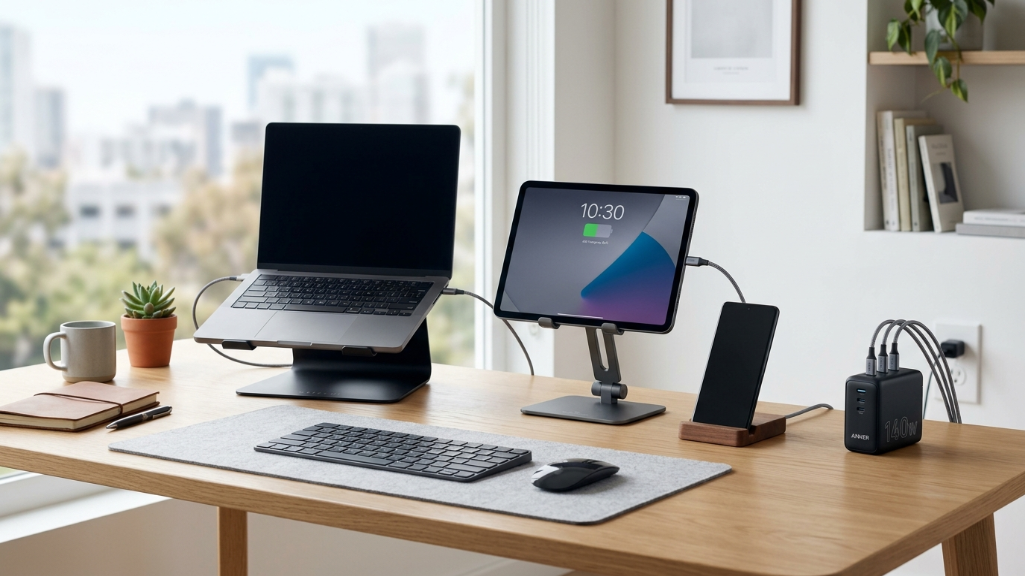
Modern usage scenarios are extremely demanding: laptops rendering video at full load, with a low-battery tablet and the latest smartphone plugged in simultaneously.
A single 140W output port is merely the baseline. The real challenge lies in how the underlying main control chip dynamically reallocates power (Dynamic Power Allocation) across multiple devices in microseconds without causing disconnections—this is the true test of the board’s architectural design.
Full-Protocol Compatibility: Engineering Depth and Hidden Barriers
Many people think buying a reference design will automatically solve multi-port charging protocol compatibility. This is a typical novice misunderstanding.
Over the past 15 years in B2B consumer electronics R&D, we’ve experienced the pain of protocol interference. Early on, when our team powered up the first generation of 100W-class PCBAs in the lab, we realized that simply supporting PD3.1 was meaningless. Connecting a device requiring a non-standard fast charge would instantly drop the power to 5W. To overcome this, our hardware engineers had to rewrite the MCU logic at the lowest level.
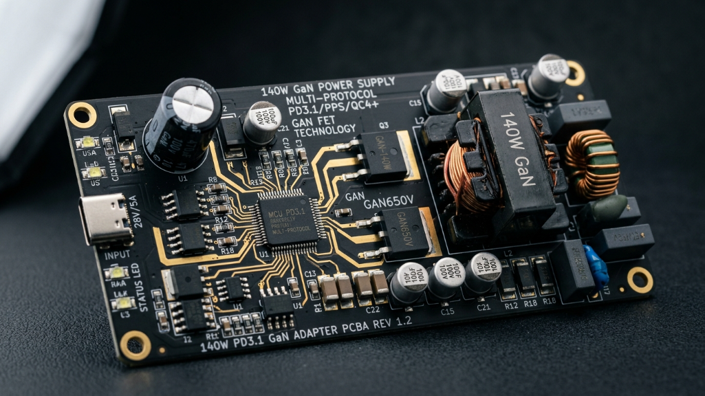
Today, our self-developed 140W PCBA architecture achieves true full-dimensional connectivity. It perfectly handshakes with PD3.0 and PD3.1, seamlessly downward-compatible with PPS, QC3.0, Huawei FCP/SCP, Samsung AFC, and even the oldest Apple 2.4A and BC1.2 protocols.
This “protocol unification” forms our unique technological moat. Below is a compatibility and handshake parameter matrix from our lab for 140W motherboards across core protocols:
| Handshake Protocol Type | Output Voltage/Current Range | Typical Devices/Scenarios | Protocol Compatibility Challenges & Our Solutions |
|---|---|---|---|
| PD 3.1 (EPR) | 28V/5A (140W) | Flagship ultrabooks / gaming laptops | Small capacitor voltage margin at 28V high voltage; we use customized high-frequency planar transformers to reduce leakage inductance loss. |
| PPS (Programmable Power Supply) | 3.3V–21V / 5A | Samsung S series / some domestic brands | Voltage step adjustment requires microsecond-level response; we optimize MCU algorithms to eliminate current spikes during dynamic regulation. |
| QC 3.0/4+ | 3.6V–20V / Smart Match | Traditional Android devices / mainstream peripherals | Cross-protocol switching can cause disconnection; we set up isolated protocol IC pools at the PCBA level. |
| SCP/FCP | 10V/4A, 5V/4.5A | Huawei ecosystem devices | High-current, low-voltage output causes heat accumulation; we use pure copper heatsinks with custom PCBA layouts to disperse heat sources. |
| Apple 2.4A / BC1.2 | 5V/2.4A (max) | Older iOS / low-current devices | D+/D- pin conflicts; we incorporate hardware-level smart recognition and shunt impedance in the PCB design. |
This is why experienced overseas clients always request a protocol compatibility test report first. Without this foundational capability, a charger is just a “charging head,” not a “smart fast-charging hub.”
Common Pitfalls When Sourcing High-Power Charger PCBAs
As a seasoned operator of OEM fast-charging PCBAs, I’ve seen countless overseas procurement managers face total collapse with their first batch. The pitfalls usually focus on two fatal points. Provide you with safe fast charging PCBA wholesale: 140W GaN guide.
Uncontrolled Heat & Safety Risks
Thermal management is a baseline requirement. Designs without sufficient temperature margin are essentially dangerous.
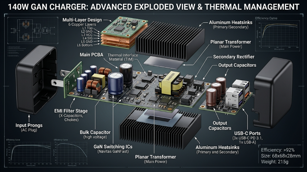
At 140W (typically using PFC+LLC or PFC+AHB architectures), even a tiny fraction of conversion efficiency loss becomes substantial heat. Many GaN charger circuit board designs work in open lab conditions but fail once enclosed in a high-density PCBA casing, causing yields to plummet. Exceeding safety temperature thresholds (e.g., case >70°C) drastically shortens capacitor life or even causes MOSFET thermal breakdown.
For our 140W boards, we abandoned simple surface-mounted heatsinks. To minimize thermal rise, we use space-grade potting combined with brass-wrapped heatsinks and asymmetrically thickened copper traces on the PCB, reducing full-load temperature by 8–10°C. These invisible costs determine whether a product gains reputation or faces mass returns.
The Gap Between Resellers and True Source Factories
The second trap is engaging the wrong party.
Walk through Shenzhen or Dongguan, and you’ll see many claiming to be “source factories.” But when you inquire about mold timelines, capacitor brands on the BOM, or request to inspect SMT machines, they dodge. These are typical trading companies—they buy bare PCBAs from Factory A, standard enclosures from Factory B, and assemble in a workshop. The supply chain is fragile; a 0.2mm deviation in an enclosure can stress the PCB, causing solder defects. Issues are blamed upstream while buyers suffer months of delays.
A true B2B consumer electronics source factory operates vertically. From the moment the hardware design is finalized, we know exactly what casing material matches the board. This is not bragging—it’s a moat built on lessons learned.
Five Core Criteria to Evaluate Fast-Charging Manufacturers
To find a factory worthy of bulk orders, ignore glossy PPTs. Focus on these five hard indicators. They are not just an industry audit guide but the survival rules we, AOVOLT, have followed in Dongguan electronics manufacturing for 15 years.
Deep Industry Experience
There is no fast track in electronics. A team that has only done 18W chargers for two years will likely burn through boards attempting a 140W project. Our 15 years in consumer electronics manufacturing cover iterations from traditional linear power to high-frequency GaN architecture. Engineers can diagnose issues by glancing at waveform charts; this intuition is invaluable.
Asset-Heavy Vertical Integration
Do not let outsourcing compromise quality. Top-tier manufacturers don’t stop at PCBA assembly.
AOVOLT pursues asset-heavy vertical integration—from advanced design to in-house R&D, mold opening, injection molding, and final assembly of metal parts and PCBA. All production elements are controlled internally.
Example: If a Type-C port on the PCBA doesn’t perfectly match the enclosure, the feel degrades and solder pads may tear. In our custom injection molding, mold engineers and PCBA layout engineers work in the same office, achieving mold precision near 0.02mm, preventing assembly errors at the source.
Premium Industrial Design (ID) Capability
On Amazon or offline channels, if your charger looks identical to competitors’, the only path is price competition.
Brands seek factories with distinctive design capabilities. Our ID team merges CMF (color, material, finish) with high-density PCBA stacking, using advanced techniques like micro-arc oxidation, laser engraving, and liquid silicone encapsulation to make a 140W industrial product feel like a luxury watch, enabling clients to achieve 30%+ brand premium.
Rigorous Standardized QC & Rapid Delivery
B2B clients fear delayed delivery more than pricing errors.
In AOVOLT’s cleanroom, every high-power board undergoes an 8-hour full-load 140W burn-in test—100% inspection, not sampling. Coupled with our efficient supply chain, even during peak cross-border e-commerce seasons, we deliver reliably.
End-to-End OEM/ODM Custom Services

From BOM cost optimization for target markets, country-specific plug certifications, to custom packaging, true source factories provide complete solutions, not just a few boards.
Why Top Cross-Border Brands Choose Vertical Integration
The underlying logic: cost and speed.
Structural Cost Reduction from Closed-Loop Production
Outsourcing multiple suppliers seems cheaper but ignores hidden costs: high communication overhead, delays, and higher defective rates.
As a vertically integrated laptop fast-charger OEM, we internalize all profit nodes, offering competitive pricing even with premium GaN switches.
| Key Stage | Traditional Multi-Party Supply Chain | Vertical Integration (AOVOLT) | Core Difference |
|---|---|---|---|
| First PCBA Sample | 15–20 days | 7–10 days | Internal team directly sends drawings to SMT without waiting for outsourcing schedules |
| Enclosure Mold & Injection | 30–45 days (frequent mold modifications) | 15–20 days (one-shot molding) | Mold and PCBA design synchronized internally, avoiding structural conflicts |
| Trial Production Defect Rate | 5–12% (assembly tolerance issues) | <1% (precise fit) | Closed-loop system locks part tolerances at source |
| Exception Handling | 3–5 days (multi-party blame) | <24 hours (internal traceability) | Single responsible party, internal engineers locate issues immediately |
Breaking Conventional Time-to-Market
Seizing market share by even a week can be decisive. While competitors wait for enclosure modifications, our first batch of 140W branded chargers is already shipped. Vertical integration gives you this “dimensionality reduction” advantage.
FAQ
Q1: Why do some 140W chargers disconnect the first device when plugging in a second?
A: The multi-channel MCU on the PCBA reallocates power too slowly or lacks a soft-start circuit. Our upgraded dual-core architecture achieves true microsecond-level seamless switching.
Q2: What core architecture does your 140W PCBA use?
A: We offer PFC+LLC (max efficiency, ultra-low heat) and PFC+AHB (compact size) GaN architectures based on client needs.
Q3: Can you work with our own ID design, handling only internal circuitry and mold production?
A: Yes. Provide 3D designs and dimensions, and we reverse-engineer high-density PCBA stacking and mold production internally.
Q4: Can your factory assist with UL, CE, FCC certifications?
A: Standard. Our PCBA design includes sufficient EMC and electrical isolation margin, achieving high pass rates on certification tests.
Q5: What are MOQ and standard delivery lead times?
A: For customized high-power OEM projects, MOQ starts at 3,000 units. Standard bulk production takes 25–30 days with materials ready.
From power banks to magnetic chargers and extreme fast-chargers, the hardware logic remains: whoever controls every pixel from code to mold wins the B2B game. If you’re seeking a Dongguan factory that truly understands low-level tech and can flawlessly execute your design, or your team is struggling with multi-port protocol compatibility and thermal management, now is the time to re-evaluate your supply chain. Send us your specifications and let’s see how source-level technology can maximize your brand’s profit margin.